Quantcast
Channel: Cadence Digital Implementation Forum
Viewing all 1453 articles
Browse latest View live

Hierarchical Synthesis in Genus

$
0
0

Hi all!

I'm trying to split a design during synthesis in order to implement a recurring subpart only one and then re-use it in cloned partitions in Innovus.

After searching the support site, I could solve the first problem: Extracting the subdesign.

My toplevel design is ControlBlock, which contains several (later hundreds) of instances of DoubleColumn.

set_db init_power_net VDD
set_db init_ground_net GND

::read_hdl -sv {
[…]
}

read_mmmc full.mmmc

read_physical -oa_ref_libs { … }

elaborate ControlBlock

set_db [get_db modules DoubleColumn*] .boundary_opto strict_no

init_design

create_derived_design {hinst:ControlBlock/gen_dcol[0].dc_I}
vcd design:DoubleColumn

syn_generic
syn_map

set_db write_sv_port_wrapper true

# write all formats that I can think of, to find one I can work with
write_design -innovus -hierarchical -base_name designs/DoubleColumn
write_db -common dbs/DoubleColumn
generate_ilm -basename ilms/DoubleColumn

At this stage, the proposed solution¹ changes back to the top design and performs synthesis there:

vcd

set_db design:DoubleColumn .preserve true

change_link -retain_exceptions -instances {hinst:ControlBlock/gen_dcol[0].dc_I} {hinst:ControlBlock/gen_dcol[1].dc_I} -design DoubleColumn

vcd design:ControlBlock

syn_generic
syn_map

write_db -common dbs/merged

However,

  • this seems to again synthesize the submodule. (Why? It's marked "preserve")
  • Constraints to FFs within the submodule are lost. I only get "No paths found" when I query timing to a FF.
  • I might want to completely split out the submodule synthesis to be done at another time.

At this stage I'm stuck at the moment. I do have all the bits and pieces (netlists, SDC, etc), but just can't find the way to combine them.

I can read the toplevel, define the ILM and assemble the design. But that does not bring in the full netlist of the subdesign, which is not contained in the ILM.

I tried starting a new session, reading the DB of the toplevel and then calling create_design to create a second design to try and bring DoubleColumn in from the DB. But this fails when reading the LEFs (Lef files are read when design exists. [PHYS-6187]). I could probably modify the DB to skip reading the physical data by patching the files. But that seems wrong to me.

In principle, I do not care whether assembly takes place in Genus or Innovus, so any solution would be appreciated.

Thanks,
Michael

My sources so far:
¹ https://support.cadence.com/apex/ArticleAttachmentPortal?id=a1O0V000009ESqVUAW&pageName=ArticleContent
² https://support.cadence.com/apex/ArticleAttachmentPortal?id=a1O3w000009xyaIEAQ&pageName=ArticleContent


Convergence issue while simulating CNTFET adder

$
0
0

Sir,

I'm working on CNTFET-based arithmetic circuits. Initially, I developed all the basic ternary logic gates using 45nm CNTFET and they were working correctly. But when I tried to simulate a half-adder, using the same, it threw an error. The total transient analysis time was 10 us, but the simulation ran only up to 2 us. Kindly help me in rectifying the same. FYI, CNTFET was a VerilogA model and it was imported into Virtuoso. 

 Error:

Error found by spectre at time = 2.017 us during transient analysis `tran'.

    ERROR (SPECTRE-16192): No convergence achieved with the minimum time step specified. 

Cannot restore design from OA databse

$
0
0

Dear community

We recently switched from a LEF-file-based design flow to a OA-based flow in Innovus 21.10. After each design step, we store the current design as OA database. For example, after the routing step, we use

saveDesign -cellview {myLibrary myDesign route}

to store the design.

Afterwards, when trying to restore the design, we get an error message saying that the import of the OA database has failed. The terminal output looks as follows:


% Begin Load MMMC data ... (date=05/03 11:25:39, mem=1281.6M)
**ERROR: (TCLCMD-989):    cannot open SDC file '<path to working directory>/myLibrary/myDesign/route#2etmp/mmmc/modes/functional_mode/functional_mode.sdc' for mode 'functional_mode'


ERROR:


    while executing
"error $catchMsg"
    (procedure "restoreDesign" line 33)

The characters above in bold are wrong, i.e. this path does not exist. The folder is simply called route, not route#2etmp. Innovus adds some non-existent characters in the path for some reason.

Looks like an issue with special characters or so (#2e gets translated to a dot in a design browser). How to fix this problem?

Some additional information that might be helpful:

  • The problem occurs in a current session (using freeDesign) as well as in a new session.
  • Manually changing the directory's name to "route#2etmp" actually fixes the problem. This is just a workaround, though.

Pin assignment

$
0
0

Hi,

I have two groups of pins for the LEFT and RIGHT sides. I have 2 problems relating to the code below.

  1. The pins appear ok in the GUI, but the spacing seems to be set to 3.2, not 2.5 as expected. Min width is not 3.2um
  2. the LEFT and RIGHT pins are not aligned in y-dim. I tried to align them using offsetStart, but that didn't work.

Many thanks for the assistance.

set interface_pin_pitch 2.5
set pin_width 0.5

editPin -pin $interface_pins\
-layer $interface_layer\
-fixedPin 1 \
-edge 2 \
-offsetStart [expr$interface_pin_pitch/2] \
-spacing $interface_pin_pitch\
-spreadType CENTER \
-pinWidth $pin_width\

editPin -pin $addr_pins\
-layer $interface_layer\
-fixedPin 1 \
-edge 0 \
-spacing $interface_pin_pitch\
-spreadType CENTER \
-pinWidth $pin_width\

2D registers

$
0
0

Hi,

I have a 2D register. Before synthesis it looks like this

moduleSPI
(
...
outputlogic [7:0] REG_DATA [7:0]
);

After synthesis it gets flattened like this:

moduleSPI(... REG_DATA);
...
output [63:0] REG_DATA;
I need to keep track of each 2D register name to make routing easier later, so how would I change this to synthesize into something more usable like the following?
output [7:0] REG_DATA0;
...
output [7:0] REG_DATA7;

DIsable writing netlist in binary format

$
0
0

I'm implementing a design with the stylus hierarchical flow. At one point, the flow fails with

**ERROR: (IMPSER-507): Error in loading binary netlist file …/PARTITION/dbs/DoubleColumn/vbin/DoubleColumn.v.bin_7.

Which is a rather obvious error, because only the files .v.bin, .v.bin_lib, and v.bin_0 to v.bin_6 actually do exist. No _7 to be found anywhere.

Note: The database was created just minutes earlier with the very same version of Innovus (from within the generated flow template). It's rather suprising that it cannot read it's own output.

It's impossible for me to debug from here to move on with the flow. My first step would be to try and disable the use of the binary format, because a plain Verilog file seems a lot easier to handle for humans. Maybe reading that could show some obvious error.

Is there some (probably hidden) flag/option to go back to using plain text files? I'm using v21.17-s075_1,.

Thanks,
Michael

Innovus: How to Query PG Via Grid information?

$
0
0

I'm using innovus tool and I'm getting a stuck when I try to get PG via grid information of the design but I dont know how to do it.

below picture shows PG via grid is the "blue line" but I can't select it. I use command: get_snap_grid_info -type but have no type corresponding to PGViaGrid. Anybody can help me please?

ERROR: (IMPSP-9099): Scan chains exist in this design but are not defined for xx% flops

$
0
0

Hi there,

I have a small design (basically a counter) which latches the output to multiple different registers at time.
So I guess that Genus is using Scan FFs with their Enable input to select the active output FFs.

The use of those FFs with Scan functionality causes Innovus to fail:

ERROR: (IMPSP-9099): Scan chains exist in this design but are not defined for 54.84% flops

However, when I forbid genus to use them by 
set_db use_scan_seqs_for_non_dft false
then it works fine but my design becomes 50% larger. 

So I don't want to do it, but how can I route the design in innovus then? It it sort of strange, doing this for 15 years now but never had this issue.

It sais it has DFFs with scan functionality, but there is no scan chain defined. So I can't delete it, because there is non...

Thanks for any hints,
 Joachim


Innovus ignores set_false_path constraint

$
0
0

Dear community

I have a design using several memories with an ECC block. There is a combinatorial path from the RAMs output to their own input through the ECC block (essentially a loop around the RAM). This path has no functional purpose und is never used in a meaningful way. Due to the large hold times of the RAMs, these loops always result in hold violations that Innovus cannot fix. Therefore, I would like to constrain them as false paths.

Each RAM consists of two blocks (left and right) each with a 39-Bit input bus (DR and DL), and a 39-bit output bus (QO and QL). In my SDC files, I use

set_false_path -from [get_pins my_mems/i0_RAM/Q*] -to [get_pins my_mems/i0_RAM/D*]

to constrain this.

Unfortunately, Innovus ignors this during timing analyses, i.e. it still reports hold violations on those paths. There is no error during the SDC file import and if I execute the command

get_pins my_mems/i0_RAM/Q*

in my Innovus shell, then I get the correct list of all 2x39 pins returned. Afraid that this might be a syntax problem, I also tried to explicitly write out all possible combinations, i.e. something like this:

set_false_path -from [get_pins my_mems/i0_RAM/QL[0]] -to [get_pins my_mems/i0_RAM/DL[0]]
set_false_path -from [get_pins my_mems/i0_RAM/QL[0]] -to [get_pins my_mems/i0_RAM/DL[1]]
set_false_path -from [get_pins my_mems/i0_RAM/QL[0]] -to [get_pins my_mems/i0_RAM/DL[2]]
...
set_false_path -from [get_pins my_mems/i0_RAM/QR[38]] -to [get_pins my_mems/i0_RAM/DR[38]]

This also does not work; Innovus still reports hold violations on those paths. Why is the tool ignoring those constraints? How to fix this?

How to resolve clock gating hold checks (nets could not be fixed because it is clock net)?

$
0
0

Dear community

I have a design with some unfixable hold violations. After the post-CTS optimization, I get the following output in the log file:

=======================================================================
                Reasons for remaining hold violations
=======================================================================
*info: Total 23 net(s) have violated hold timing slacks.

Buffering failure reasons
------------------------------------------------
*info:    23 net(s): Could not be fixed because it is clock net.

Resizing failure reasons
------------------------------------------------
*info:    23 net(s): Could not be fixed because it is clock net.

When I open the timing debugger, these violations are entitled as clock gating hold checks, which are described here.

If I run

report_timing -check_type clock_gating_setup -max_paths 23

then there is plenty of positive setup slack remaining. What could prevent the tool from fixing thos violations?

Thank you for any advice.

Innovus vs Calibre DRC results

$
0
0

Dear all, 

I have a DRC-clean design on Innovus (verified by the Innovus tool: Verify -> Verify DRC). However, when I extract the GDS and import it into Calibre, hundreds of errors are highlighted! Calibre uses a separate DRC_rule_file which, I think, Innovus has no access to.
I guess Innovus only uses the rules in the .LEF files to generate and verify the layout, am I right?
Is it possible to feed the DRC_rule_file (what Calibre reads) to Innouvs so the generated layout meets those rules?
Should I trust Innovus and go ahead with the current design?
Could it be an issue with generating the GDS file? 

Many thanks,

Anas

Cadence genus synthesis

$
0
0

Hi all,

After doing Synthesis using Genus i am getting "No Unconstrained paths found" in  the generated timing report. And also in QOR report in cost group only clock paths are identified, No other paths are coming. So please help me identifying the issue.

Thanks in advance

Are the -add and -master_clock constraints needed in an MMMC setup?

$
0
0

Dear community

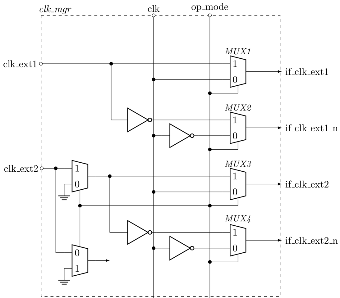
I am working on a design that distinguishes between six different operational modes in its MMMC setup, i.e. there are six different SDC files. For simplicity, let us assume that there are only two modes: the normal mode and the test mode. Please consider the following circuit diagram of a module called clk_mgr:

Whether or not the design is in its normal mode is decided by the external signal op_mode. If this signal is logical 1 then the design is operating in the normal mode. It operates in the test mode otherwise.

The instance clk_mgr outputs four clocks. In the normal mode, they are driven by their respective clock input. In the test mode, all four are driven by the main clock clk. clk_ext1 and clk_ext2 are additional, external clocks running at a lower frequency. The special thing about clk_ext2 is that its pin is shared, i.e. in the test mode, no clock signal is applied to that pin; instead, it becomes a normal data path.

When a pin can be driven by multiple clock signals, textbooks suggest to define both clocks using the -add argument. For example, one could define the clock at if_clk_ext1 as follows

create_clock -name "if_clk_ext1_normal" -period 62.2 [get_pins MUX1/Q]
create_clock -name "if_clk_ext1_test" -period 83.3 [get_pins MUX1/Q] -add

Alternatively, one can define a generated clock. Here, the master_clock argument is used to specify which of the clocks reaching the specific source object should be used for deriving the characteristics of the generated clock:

create_clock -name "clk" -period 62.2 [get_ports clk]
create_clock -name "clk_ext1" -period 83.3 [get_ports clk_ext1]
create_generated_clock -name "if_clk_ext1_normal" -divide_by 1 -source [get_ports ???] -master_clock clk [get_pins MUX1/Q]
create_generated_clock -name "if_clk_ext1_test" -divide_by 1 -source [get_ports ???] -master_clock clk_ext1 [get_pins MUX1/Q] -add

The textbook examples I can find usually use sequential elements to define their clocks - not combinatorial elements like MUXs as in my example. Hence, I am unsure what to put as the source object (as inicated by the 3 question marks). Using [get_ports clk] and [get_ports clk_ext1], which might be the most reasonable option, seems redundant to me. Also, the master_clock argument might not be needed at all in this case.

For purely combinatorial paths, there is also the -combinational argument which could be used as follows:

create_clock -name "clk" -period 62.2 [get_ports clk]
create_clock -name "clk_ext1" -period 83.3 [get_ports clk_ext1]
create_generated_clock -name "if_clk_ext1" -combinational -source [get_ports clk] [get_pins MUX1/Q] # normal mode
create_generated_clock -name "if_clk_ext1" -combinational -source [get_ports clk_ext1] [get_pins MUX1/Q] # test mode

Here, my understanding is that the -add option does not work.

Whether any of these 3 options is correct I do not know. Also, is any of this necessary when there are multiple SDC files as in a MMMC setup?

Here is how I would constrain this design:

SDC file of the normal mode

set_case_analysis 1 [get_ports op_mode]
create_clock -name "clk" -period 62.2 [get_ports clk]
create_clock -name "clk_ext1" -period 83.3 [get_ports clk_ext1]
create_clock -name "clk_ext2" -period 250.0 [get_ports clk_ext2]
create_generated_clock -name "if_clk_ext1" -divide_by 1 -source [get_ports clk_ext1] [get_pins MUX1/Q]
create_generated_clock -name "if_clk_ext1_n" -divide_by 1 - invert -source [get_ports clk_ext1] [get_pins MUX2/Q]
create_generated_clock -name "if_clk_ext2" -divide_by 1 -source [get_ports clk_ext2] [get_pins MUX3/Q]
create_generated_clock -name "if_clk_ext2_n" -divide_by 1 - invert -source [get_ports clk_ext2] [get_pins MUX4/Q]

SDC file of the test mode

set_case_analysis 0 [get_ports op_mode]
create_clock -name "clk" -period 62.2 [get_ports clk]
set_input_delay -clock [get_clocks clk] -add_delay 5.0 [get_ports clk_ext2]
create_generated_clock -name "if_clk_ext1" -divide_by 1 -source [get_ports clk] [get_pins MUX1/Q]
create_generated_clock -name "if_clk_ext1_n" -divide_by 1 - invert -source [get_ports clk] [get_pins MUX2/Q]
create_generated_clock -name "if_clk_ext2" -divide_by 1 -source [get_ports clk] [get_pins MUX3/Q]
create_generated_clock -name "if_clk_ext2_n" -divide_by 1 - invert -source [get_ports clk] [get_pins MUX4/Q]
Technically, the tool should be able to infer the correct clock source based on the operational mode and the set_case_analysis constraint, right? Also notice that clk_ext2 gets an input delay constraint since it is a normal data path now. 
I would be thankful for an explaination on which solution is correct and why.

How to prevent sroute from placing vias where there already are some?

$
0
0

Dear Community

Please consider the following screenshot:

The image shows part of the power grid (MET5 horizontal and MET6 vertical) and a RAM block surrounded by a block ring. The RAM's power pins (horizontal stripes above the block) are connected to its ring.

When I execute

setSrouteMode -viaConnectToShape {ring stripe blockring}
sroute -connect {corePin} -corePinTarget {ring blockring stripe} -nets {vddd vssd} -allowLayerChange 1 -allowJogging 0

The following result occurs:

The second image shows a close-up of the righ-hand side of the block ring. Since the standard rows are not necessarely aligned with the power pins of the RAM, it can occure the core pins cannot made a direct connection to the power grid. sroute now places a second via stack, i.e. the via stack from the RAM's power pins and the one from the standard row are overlapping, causing a design rule violation.

Strangely, this only occurs at block rings. There are other situations in the design where the place for a direct via stack is already occupied by something else. For example, power pads that are connected to the core ring. In these cases, sroute simply stops in front of them and places no vias, i.e. it leaves the ends open. They can then be later routed using the -allowJogging 1 argument.

Is there a simple way to prevent these design rule violations? Or is there a command that tries to merge overlapping via stacks?

Thank you.

Instance grid not aligned to core sites due to automatic changes on the floorplan made by Innovus

$
0
0

Dear community

When I load my floorplan (as .def file) into Innovus 21.10, I get the following message in the log:

floor plan core box changed from {{160.160000,160.160000},{3393.040000,3822.000000}} to {{31.560000,31.550000},{3519.400000,3951.920000}}

This changes the distance from the core to the IO boundary. As a result, the core box is no longer an integer multiple of the pitch size away from the origin, resulting in an instance grid that is not aligned to the core sites. See pictures below:


Why does that happen and how to prevent it?

Some additional information:

1. The core box is not explicitly defined in our DEF File. All it does is defining the die area and the rows of the standard cells and I/O pads. Here is an excert from the .def file (only the relevant part):

VERSION 5.7 ;
DIVIDERCHAR "/" ;
BUSBITCHARS "[]" ;

UNITS DISTANCE MICRONS 1000 ;
PROPERTYDEFINITIONS
  DESIGN CatenaDesignType STRING "asic" ;
  DESIGN lastSavedExtractCounter INTEGER 178670 ;
END PROPERTYDEFINITIONS

DIEAREA ( 3553000 2468000 ) ( 3236000 2468000 ) ( 3236000 3982000 ) ( 3087000 3982000 ) ( 3087000 3177000 ) ( 2457000 3177000 ) ( 2457000 3832000 ) ( 2115000 3832000 ) ( 2115000 3982000 ) ( 2011000 3982000 ) ( 2011000 3832000 ) ( 1198000 3832000 ) ( 1198000 3982000 ) ( 1068000 3982000 ) ( 1068000 2015170 ) ( 334160 2015170 ) ( 334160 1619970 ) ( 1068000 1619970 ) ( 1068000 598120 ) ( 382000 598120 ) ( 382000 305000 ) ( 0 305000 ) ( 0 0 ) ( 3553000 0 ) ;
ROW Row_0_1 io_site_F3V 3393000 160000 W DO 1 BY 2308 STEP 0 1000 ;
ROW Row_0_1_2 io_site_F3V 0 0 N DO 3393 BY 1 STEP 1000 0 ;
ROW ROW_3 core_hdll 35840 208320 N DO 5704 BY 1 STEP 560 0 ;
ROW ROW_4 core_hdll 35840 212800 FS DO 5704 BY 1 STEP 560 0 ;
ROW ROW_5 core_hdll 35840 217280 N DO 5704 BY 1 STEP 560 0 ;
ROW ROW_6 core_hdll 35840 221760 FS DO 5704 BY 1 STEP 560 0 ;
[...]

2. Using something like changeFloorplan -coreToBottom 30 completely screws up the floorplan and makes it unusable.

3. Exporting the floorplan after making some changes to the core box adds the following information to the .def file:

PROPERTYDEFINITIONS
    DESIGN lastSavedExtractCounter INTEGER 178670 ;
    DESIGN CatenaDesignType STRING "asic" ;
    COMPONENTPIN designRuleWidth REAL ;
    DESIGN FE_CORE_BOX_LL_X REAL 31.5600 ;
    DESIGN FE_CORE_BOX_UR_X REAL 3519.4000 ;
    DESIGN FE_CORE_BOX_LL_Y REAL 31.5500 ;
    DESIGN FE_CORE_BOX_UR_Y REAL 3951.9200 ;
END PROPERTYDEFINITIONS

Copy-pasting these FE_CORE_BOX_* lines into my own floorplan and changing the numbers to the correct values also results in an unusable floorplan that is screwed up.


No buffers added in power domain, hold violation

$
0
0

I have specified two power domains, PD_CORE and PD_ACC. PD_CORE is the default and seems to work fine.
However, the second power domain, PD_ACC, causes some issues. PD_ACC is defined to a certain area, thus causing PD_ACC to have the attribute fence.

I have specified libraries for both domains, however when running CTS, I notice that no buffers or inverters are placed in this domain.
This leads to hold violations in PD_ACC, that can't be fixed since no buffers are added.

I could be incorrect, but as far as I understand this is done in the CPF, and was done as follows

-----------------------------------------------------------------------------
define_library_set -name TT_LIB -libraries $PATHS_TO_MY_LIBRARIES
set_design $init_top_cell
create_power_nets -nets {VDD_NET VDD_ACC}
create_ground_nets -nets {VSS_NET}
create_power_domain -name {PD_CORE} -default
update_power_domain -name PD_CORE -primary_power_net VDD_NET -primary_ground_net VSS_NET -nmos_bias_net VSS_NET -pmos_bias_net VDD_NET
create_power_domain -name {PD_ACC} -instances $ACC_INST
update_power_domain -name PD_ACC -primary_power_net VDD_ACC -primary_ground_net VSS_NET -nmos_bias_net VSS_NET -pmos_bias_net VDD_ACC
create_nominal_condition -name TT -voltage 0.80
update_nominal_condition -name TT -library_set "TT_LIB"
create_power_mode -name PM_0P80 -domain_condition {PD_CORE@TT PD_ACC@TT} -default

<creating global conditions>
..
end_design
-----------------------------------------------------------------------------

In cc_opt_mode, I have specified the cells to be used for -cts_inverter_cells, -cts_buffer_cells, and -cts_clock_gating_cells.
The command  `get_ccopt_property buffer_cells -power_domain PD_ACC` returns the list of buffers as expected.

After running
create_ccopt_clock_tree_spec
ccopt_design -outDir RPT/innovus -prefix cts

I do `selectInstByCellName *CKBUF*, and see how buffers have been placed in all areas but the PD_ACC area - which is a bit concerning.

During `optDesign -postCTS -hold -outDir RPT/innovus -prefix -postcts_hold` i get the following

-----------------------------------------------------------------------------
**WARN: (IMPCCOPT-1182): The clock_gating_cells property has no usable full-cycle clock gates for power domain PD_ACC.
..
..
For power domain PD_ACC:
For power domain PC_CORE:

Buffers: {<list of buffers>}
Inverters: {<list of inverters>}
Clock gates: {<list of clock gates>}

-----------------------------------------------------------------------------

I assume that I am missing something crucial? I would very much be interested in finding out why the tool believes that the list of buffers, inverters and clock gates, are empty for PD_ACC, as shown in the log above.
Any help in the right direction would be appreciated!

Thank you in advance

INNOVUS 21.11

Spare cells are outside their region/fence

$
0
0

Dear Community

I use the following setup to place spare cells in my design:

createSpareModule -moduleName spare_clk_domain -cell {SDFRRHDLLX1 1 NA4HDLLX1 2 NO4HDLLX1 2 MU4HDLLX1 DLY8HDLLX1 1 BUHDLLX8 1 INHDLLX4 2} -clock clk -reset rst_n:RN -tie {LOGIC0HDLL LOGIC1HDLL}
placeSpareModule -moduleName spare_clk_domain -numModules 20
place_opt_design

After placement, when I run

checkPlace reports/placement_check.rpt

most of the spare modules cause a SPRF violation:

## Insts placed outside their region/fence (103) ##
#########################################################
### 103 Region/Fence Violation>
set pchkRegionFenceList [list \
    {spr_14/spr_gate10} \
    {spr_14/spr_gate9} \
    {spr_14/spr_gate7} \
    {spr_14/spr_gate1} \
    {spr_14/spr_gate0} \
    {spr_13/spr_gate10} \
    {spr_13/spr_gate9} \
    {spr_13/spr_gate8} \
    {spr_13/spr_gate7} \
    {spr_13/spr_gate6} \
    {spr_13/spr_gate5} \
    {spr_13/spr_gate4} \
    {spr_13/spr_gate3} \
    {spr_13/spr_gate2} \
    {spr_13/spr_gate1} \
    {spr_13/spr_gate0} \
    {spr_11/spr_gate10} \
    {spr_11/spr_gate9} \
    {spr_11/spr_gate8} \
    {spr_11/spr_gate7} \
    {spr_11/spr_gate6} \
    {spr_11/spr_gate5} \
    {spr_11/spr_gate4} \
    {spr_11/spr_gate3} \
    {spr_11/spr_gate2} \
    {spr_11/spr_gate1} \
    {spr_11/spr_gate0} \
    {spr_10/spr_gate10} \
    {spr_10/spr_gate9} \
    {spr_10/spr_gate7} \
    {spr_10/spr_gate6} \
    {spr_10/spr_gate5} \
    {spr_10/spr_gate4} \
    {spr_10/spr_gate3} \
    {spr_10/spr_gate2} \
    {spr_10/spr_gate1} \
    {spr_10/spr_gate0} \
    {spr_9/spr_gate10} \
    {spr_9/spr_gate9} \
    {spr_9/spr_gate8} \
    {spr_9/spr_gate7} \
    {spr_9/spr_gate6} \
    {spr_9/spr_gate5} \
    {spr_9/spr_gate4} \
    {spr_9/spr_gate3} \
    {spr_9/spr_gate2} \
    {spr_9/spr_gate1} \
    {spr_9/spr_gate0} \
    {spr_8/spr_gate10} \
    {spr_8/spr_gate9} \
    {spr_8/spr_gate8} \
    {spr_8/spr_gate7} \
    {spr_8/spr_gate6} \
    {spr_8/spr_gate5} \
    {spr_8/spr_gate4} \
    {spr_8/spr_gate3} \
    {spr_8/spr_gate2} \
    {spr_8/spr_gate1} \
    {spr_8/spr_gate0} \
    {spr_7/spr_gate10} \
    {spr_7/spr_gate9} \
    {spr_7/spr_gate8} \
    {spr_7/spr_gate7} \
    {spr_7/spr_gate6} \
    {spr_7/spr_gate5} \
    {spr_7/spr_gate4} \
    {spr_7/spr_gate3} \
    {spr_7/spr_gate2} \
    {spr_7/spr_gate1} \
    {spr_7/spr_gate0} \
    {spr_4/spr_gate10} \
    {spr_4/spr_gate9} \
    {spr_4/spr_gate8} \
    {spr_4/spr_gate7} \
    {spr_4/spr_gate6} \
    {spr_4/spr_gate5} \
    {spr_4/spr_gate4} \
    {spr_4/spr_gate3} \
    {spr_4/spr_gate2} \
    {spr_4/spr_gate1} \
    {spr_4/spr_gate0} \
    {spr_2/spr_gate10} \
    {spr_2/spr_gate9} \
    {spr_2/spr_gate8} \
    {spr_2/spr_gate7} \
    {spr_2/spr_gate6} \
    {spr_2/spr_gate5} \
    {spr_2/spr_gate4} \
    {spr_2/spr_gate3} \
    {spr_2/spr_gate2} \
    {spr_2/spr_gate1} \
    {spr_2/spr_gate0} \
    {spr_1/spr_gate10} \
    {spr_1/spr_gate9} \
    {spr_1/spr_gate8} \
    {spr_1/spr_gate7} \
    {spr_1/spr_gate6} \
    {spr_1/spr_gate5} \
    {spr_1/spr_gate4} \
    {spr_1/spr_gate3} \
    {spr_1/spr_gate2} \
    {spr_1/spr_gate1} \
    {spr_1/spr_gate0} \
    ]

1. I do not specify a particular area in the design for my spare cells; they are just distributed evenly by the tool. So why does this error occur?

2. How can I see/highlight/delete those fences/regions that are apparently existing?

Thank you for any suggestions.

Voltus: WARNING IMPEXT-2773

$
0
0

Hi Cadence Supporter,

I'm a newbie with Voltus.

When I'm trying to run dynamic rail analysis, I got an warning IMPEXT-2773 with the following message:

The via resistance between layers M0 and M1 could not be determined from the LEF technology file because the via resistance specification is missing. A default of 4 Ohms will be used as via resistance between these layers.

How could I do for passing this warning?

thanh you so much

Voltus: How to validate which qrc techfile is used during tool top-level power grid extraction

$
0
0

Hi Cadence Supporter,

I'm a newbie with Voltus.

When run rail analysis, we need to specify : set_rail_analysis_mode -extraction_tech_file abc.qrc

But how can we double-check the tool uses desired qrctechfile or not. Are there any dump report or something to make sure we use right qrctechfile?

thanh you so much

could not find lookup table definition

$
0
0

The extension of library is .lib and using SKY130 library .

what kind of lookup definition required?


Analyzing the design with the following configuration
-----------------------------------------------------
Design - Rev_top
Decompressor - xor
Compressor - xor
Mask - wide1
Ratio - 4 8 12

Info : A product license has been checked in. [TUI-307]
: The license name is 'Modus_DFT_Opt' a feature of DFT Modus Opt.
Error : Could not find the look-up table definition. [LBR-517]

Viewing all 1453 articles
Browse latest View live


<script src="https://jsc.adskeeper.com/r/s/rssing.com.1596347.js" async> </script>